Optimizing PCB Layout
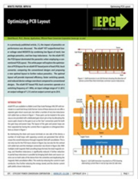
This white paper will explore the optimization of PCB layout for an eGaN FET based point of load (POL) buck converter, comparing the conventional designs and proposing a new optimal layout to further reduce parasitics.
The optimal layout will provide improved efficiency, faster switching speeds, and reduced device voltage overshoot compared to conventional designs.
Download this whitepaper to learn more.
Read More
By submitting this form you agree to Efficient Power Conversion Corporation (EPC) contacting you with marketing-related emails or by telephone. You may unsubscribe at any time. Efficient Power Conversion Corporation (EPC) web sites and communications are subject to their Privacy Notice.
By requesting this resource you agree to our terms of use. All data is protected by our Privacy Notice. If you have any further questions please email dataprotection@techpublishhub.com
Related Categories: Capacitors, Power


More resources from Efficient Power Conversion Corporation (EPC)

Improve DC-DC Flyback Converter Efficiency Using eGaN FETs
DC-DC converter designers can achieve low cost at low power densities by using flyback converters and enhancement mode gallium nitride transistors....

eGaN® FETs in High Frequency Resonant Converters
In this white paper eGaN FET technology is applied in a high frequency resonant converter. Previously, the advantages provided by eGaN FETs in hard...

eGaN® FETs for Envelope Tracking
Gallium nitride transistors can be used to improve the efficiency of DC-DC conversion.
In this white paper we look at a new application that ...
